Why Panelize
As we mentioned in article The Surprising Secret to Designing Combination Method of PCB Panels, panelization is a must-have with the consideration of PCB fabrication efficiency, reducing PCB assembly labor cost and quality control.
Panel Requirements for PCB Assembly
Wellink does PCB Assembly panel production with min size 50*50mm, max size 310*410mm. We can manufacture circuit boards based on your panelized PCB file. If you only have single PCB file, we can help panelize design according to your specific demands, then manufacture the boards. Feel free to send us a message if you need assistance in PCB Assembly panel, we'll react accordingly.
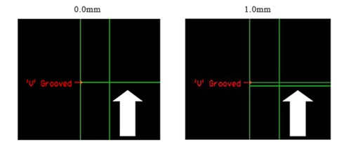
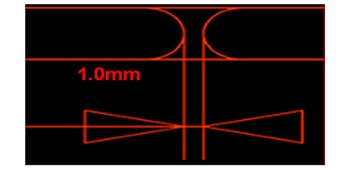
1. Panel with V-CUT/V-GROOVE
We require 0.0mm spacing between each unit for panel with V-cut, following image for your reference.
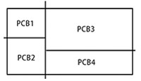
As the V-scoring could only go all through the whole board and no-stop, V-cut cannot be used for the panel with units of different size. Take the following panel for an example, we would recommend Tab-routing instead of V-cut.
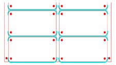
2. Panel with TAB-ROUTE
For panel with Tab-route, we need 2.0mm spacing between each unit. We offer two options for tab-routing: Tab-Route with breaking holes and Tab-route with tabs.
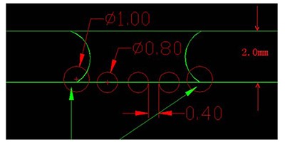
• Tab-Route with breaking holes
For this kind of Tab-route, we require breaking holes diameter be between 0.3mm-1.0mm, spacing between the breaking holes be ≥0.25mm, breaking holes number in each tab be around 5-6. See the following picture for an example.
• Tab-route with tabs, the width of tabs should be 1.0mm.
3. Panel with both V-CUT and ROUTE Fiducial
For panel with both V-cut and Route fiducial, we require 2.0mm spacing between each unit. Please refer the following image to design the panel.
Fiducial marks and mounting holes in panel
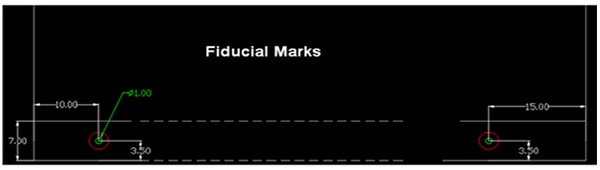
1. Fiducial marks
For each panel, we require at least 3 fiducial marks. Those marks should be placed in the middle of the tooling strips with the diameter at 1.0mm.
The fiducial marks on board's left should be 10.0mm away from the board edge, and the right ones should be 15.0mm away from the board's right edge. Following image is for your reference.
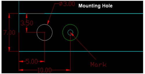
2. Mounting holes
We would recommend diameter of mounting holes to be set at 3.0mm and the width of tooling strips at 7.0mm, and at least 5.0mm distance from the edge of the board. Check the image below for reference.
Need more PCB design tips to take advantage of our assembly capabilities and lower your overall production cost and time? Check this article for practical solutions.
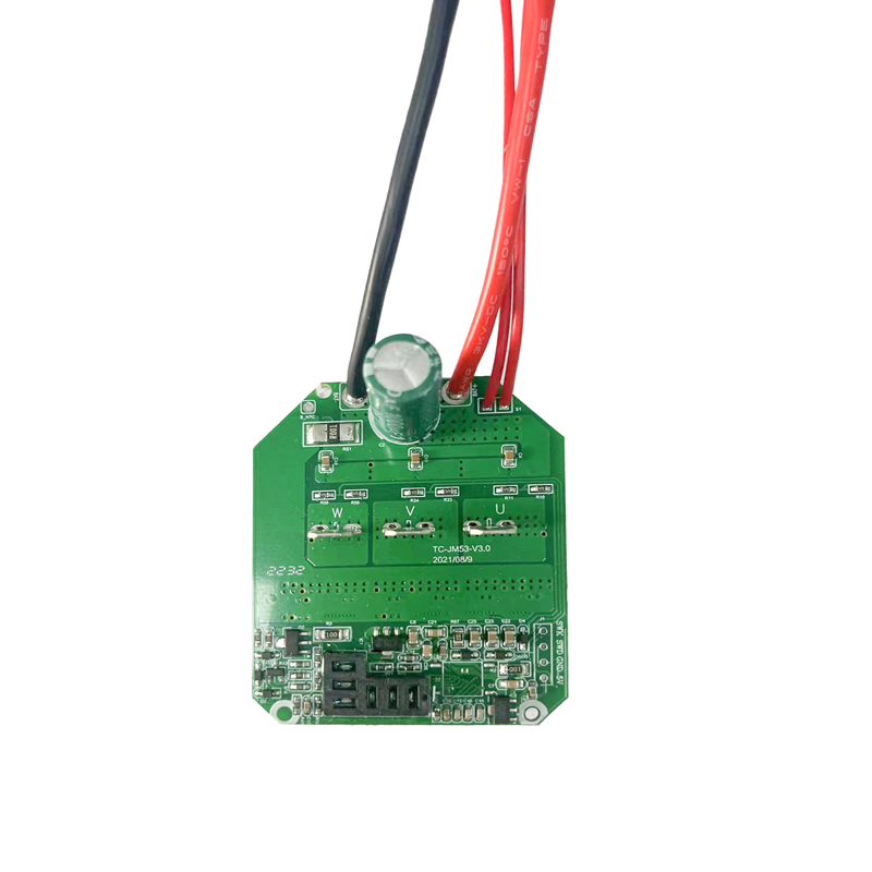
Brushless electric wrench controller parameters
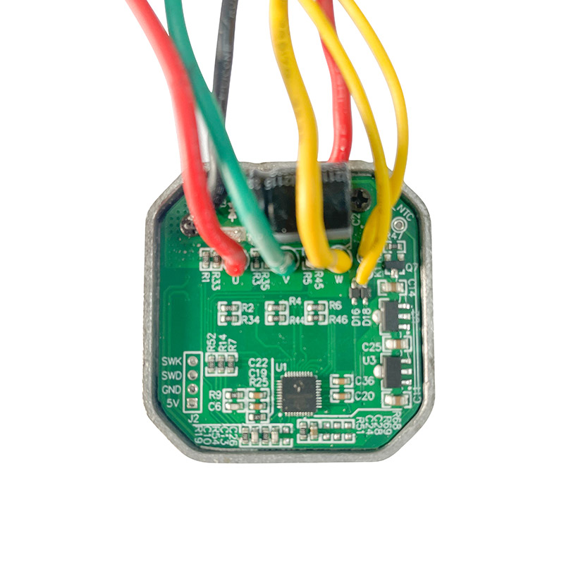
Brushless electric drill controller parameters
Brushless angle grinder controller parameters
Brushless cutting machine controller parameters
Brushless electric chain saw controller parameters
Brushless Hedge Trimmer Controller Parameters
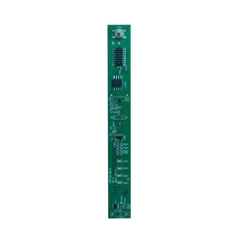
Electric toothbrush
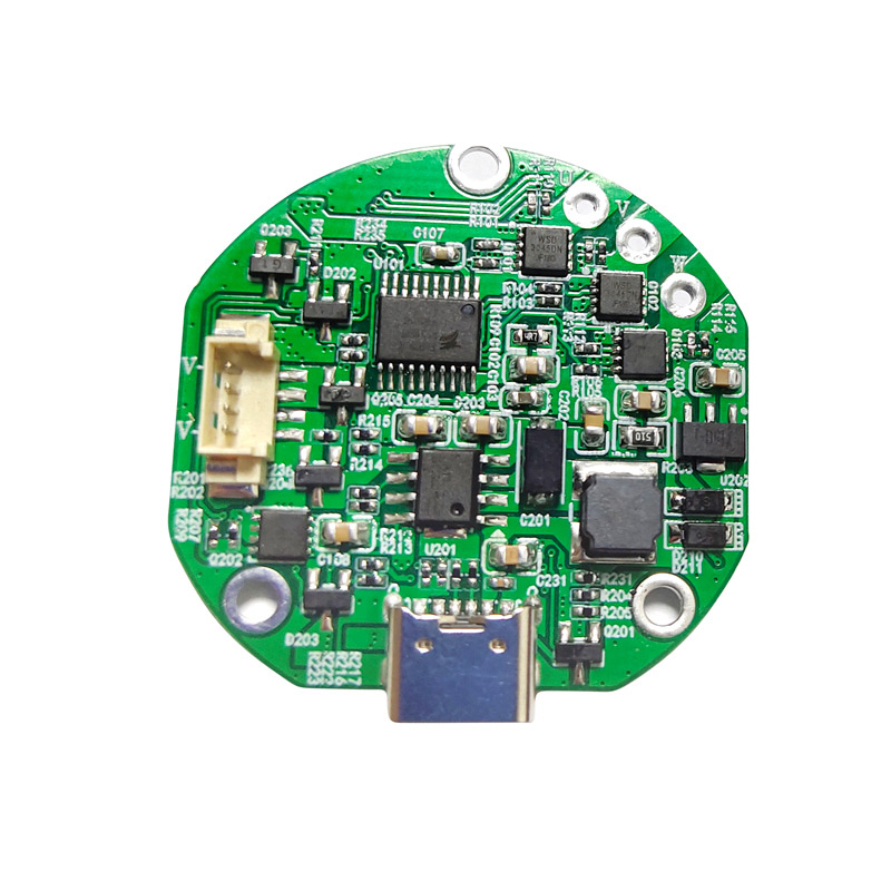
Fascia gun
B-3F, No.19 He Xing Rd, Shatou Chang'an, Dongguan 523866, China.
T: (86) 755-8657 2900
F: (86) 769-8225 4557
E: sales@efocn.com
Copyright© Wellink Industrial Tech (Shenzhen) Co., Ltd.