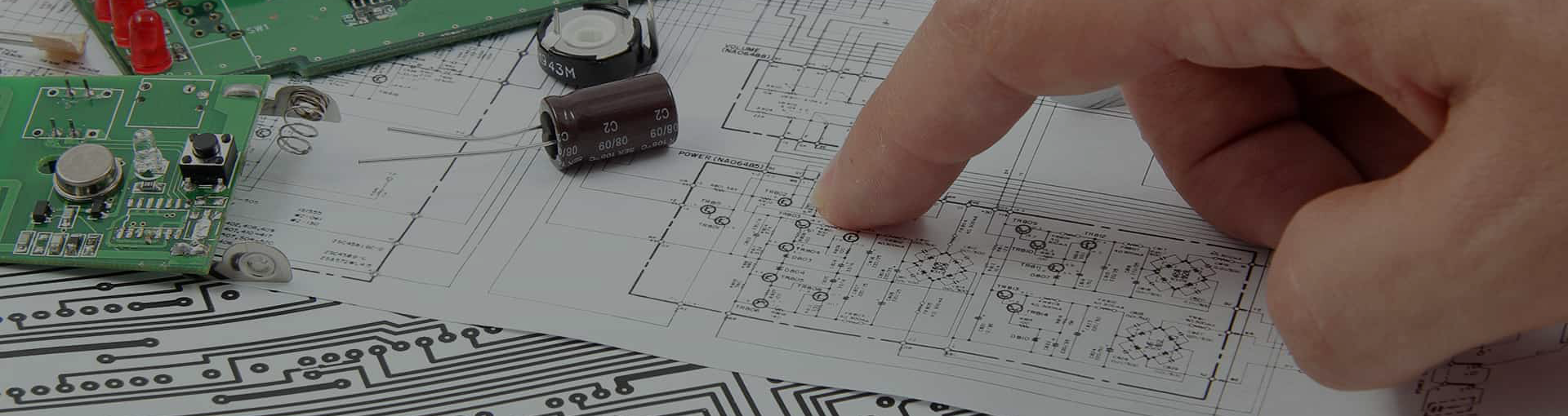
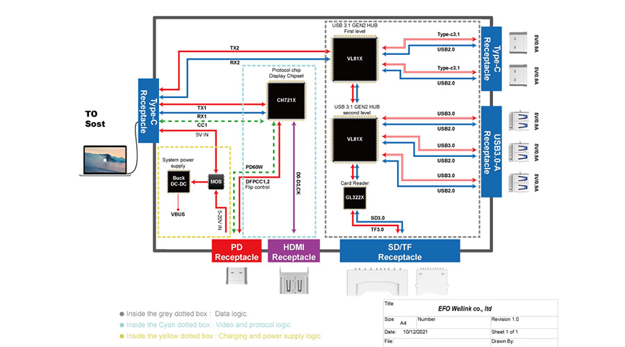
Part1: PCBA scheme design
Your time is valuable, which is why you want to design your printed circuit board correctly from the start. In our comprehensive guide, we cover everything you need to know, including PCB design basics and steps, materials and composition, best practices, and more so that you’re prepared to design the best possible printed circuit board.
PCB Design Basics
Step by Step PCB Design Guide
PCB Design Best Practices
PCB Composition & Materials
PCB Layout Capabilities
PCB and Flex Design Basics
A printed circuit board (PCB) is a flat plate or base of insulating materials that contains a pattern of conducting material and components, and some projects can be quite complex. But all PCBs have to start somewhere — and that’s with design.
Why are PCB design basics so important? Multiple extensive revisions can seriously delay the completion of your project — costing you time and money. It’s important to work with engineering experts from the beginning so that you can design for manufacturability and ensure a final, cost-effective product that works efficiently and effectively.
Step-by-Step PCB Design Guide
From the initial drawings to the final files, here are the 9 steps toward designing a printed circuit board:
1. Understand the electrical parameters.
Before starting a PCB design, you should know and understand the electrical parameters of the system, including:
● Current maximums
● Voltages
● Signal types
● Capacitance limitations
● Impedance characteristics
● Shielding considerations
● Type and location of circuit components and connectors
● Detailed net wire listing and schematic
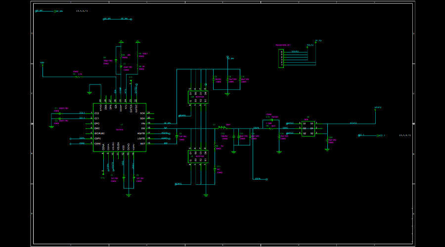
2. Creating the schematic.
One of the first steps is always creating a schematic, which refers to the design at the electrical level of the board’s purpose and function. At this point, it’s not yet a mechanical representation.
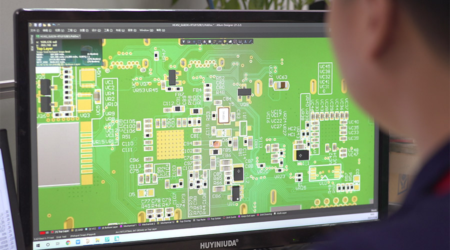
3. Use a schematic capture tool to create your PCB layout.
The right PCB provider will work with principal engineers to develop a schematic with a software platform such as Mentor PADS®, Allegro, or Altium, which shows you exactly how your board will operate and where the components will be placed. After you create your schematic, the mechanical engineer will load the design and determine how it will fit in the intended device.
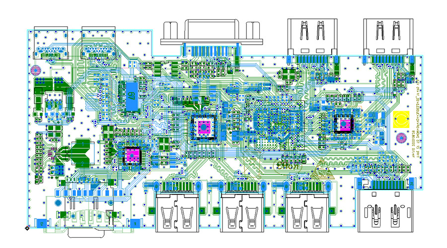
4. Design your PCB stackup.
This is important to consider early on in the PCB design stage due to impedance, which refers to how much and how quickly electricity can travel down a trace. The stackup plays a role in how the mechanical engineer can design and fit the PCB into the device.
5. Define design rules and requirements.
This step is largely dictated by standards and acceptability criteria from the IPC, which is the industry association for PCB and electronics manufacturing. These standards tell you everything you need to know regarding PCB manufacturing. An important tip: Find a PCB layout provider who is extremely familiar with IPC standards; this can help you avoid major revisions and project delays.
6. Place your components.
In many cases, the customer and PCB provider will discuss design and layout guidelines when it comes to the placement of components. For example, there may be standards indicating that certain components cannot be placed near others because they create electrical noise in the circuit. The PCB provider will have data sheets on every component (in most cases these are connectors), which will then be placed in the mechanical layout and sent to the customer for approval.
7. Insert drill holes.
This step is driven by the components and a connection. About half of the flex circuits on the market are double-sided, which means they have connection to the drill hole on the bottom layer.
8. Route the traces.
After you’ve placed the components and drill holes, you’re ready to route the traces, which means connecting segments of the path.
9. Add labels and identifiers.
Now is the time to add any labels, identifiers, markings, or reference designators to the layout. Reference designators are helpful in showing where specific components will go on the board.
10. Generate design/layout files.
This is the final step in the layout process. These files contain all the information pertaining to your printed circuit board, and once they have been generated, your PCB is now ready for fabrication and manufacturing and assembly.
PCB Design Best Practices
It’s important to communicate with the PCB or flex application engineer during the beginning of any PCB design job and discuss everything you need or require for your project. Open and constant communication with your PCB provider ensures that you’re both on the same page, which can reduce the need for multiple extensive revisions.
While it is rare that a printed circuit board is 100% perfectly designed on the first try, communication will help ensure that your PCB is properly designed from the start and that any revisions are not major ones that will derail your project and timeline.
When you submit a design, you also need to have the right board size, trace width, materials, component placement, and tolerances. Plus, in the case of flex, you’ll need to determine whether the design is static, partly flexible, or dynamic.
It’s also important to consider the environment in which the product has to function. Is the printed circuit board or flex circuit designed for a non-extreme environment, such as your cell phone, or the highest of extremes, such as an explosion?
You’ll likely have questions about the PCB design and layout process, which means it’s best to find a reputable PCB provider with extensive engineering experience who can answer your questions and ensure a smooth project from start to finish.
PCB Composition & Materials
A copper-clad substrate or polyimide-based film is often used for flex circuits, and FR4 (or an FR4 stiffener) is used for rigid-flex. FR4 allows you to build up the layers as the technology content is created.
A solder mask is also used, which is a technique where everything on the circuit board is coated with an epoxy-based LPI or cover coat for flex, except the contacts to be soldered, the gold-plated terminals of any card-edge connectors, and fiducial marks.
PCBs also include a legend application, which are the decals and reference designators in epoxy ink on a board. The name refers to the method of application in which the ink is automatically applied similar to ink jet printers
PCB Layout Capabilities
Cirexx can configure digital, analog, mixed signal technology, controlled impedance, matched length pairs DDR, RF layout, and high speed signals up to 100+ GHz for all of the following PCB structures:
● Flex circuits
● Rigid-flex circuits
● Rigid circuits
● Hybrid circuits
● BGA/micro BGA
● Blind vias
● Buried vias
● Surface mount/thru-hole/chip (die)
● High-Density Interconnect (HDI)
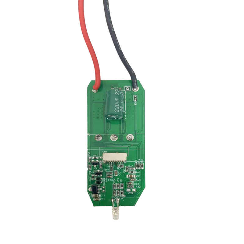
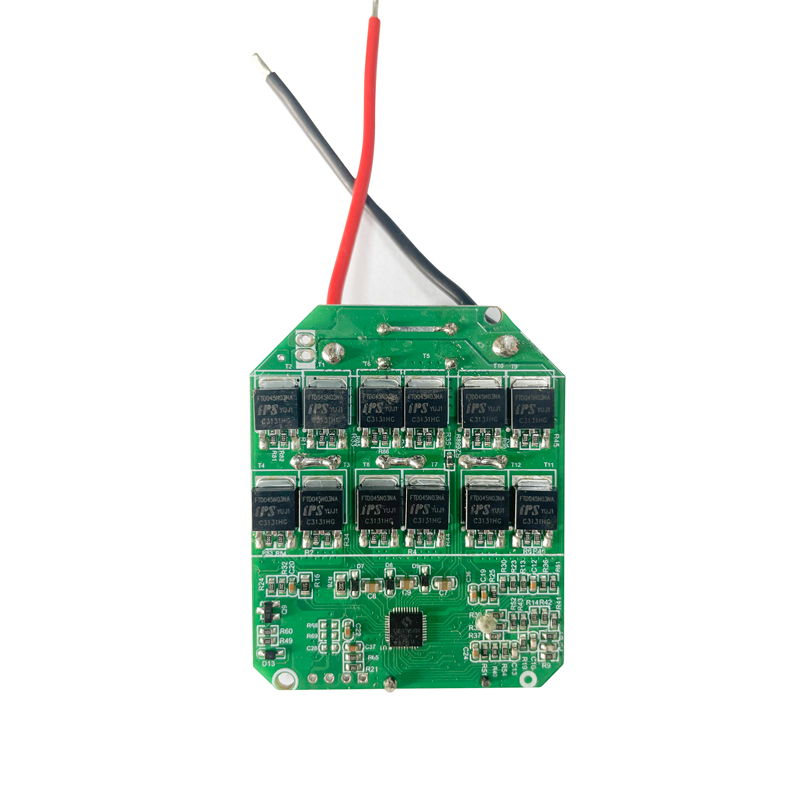
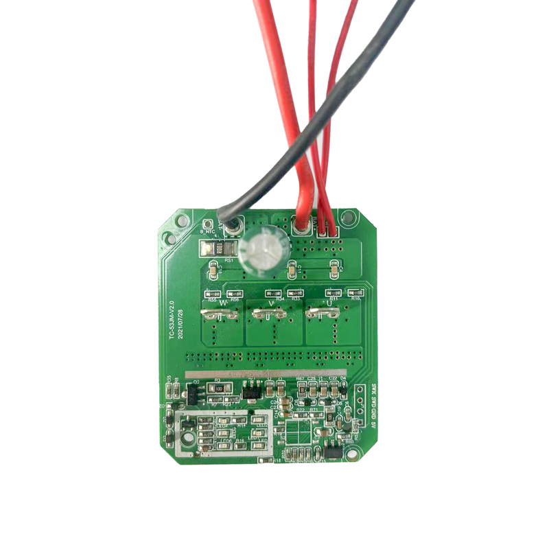
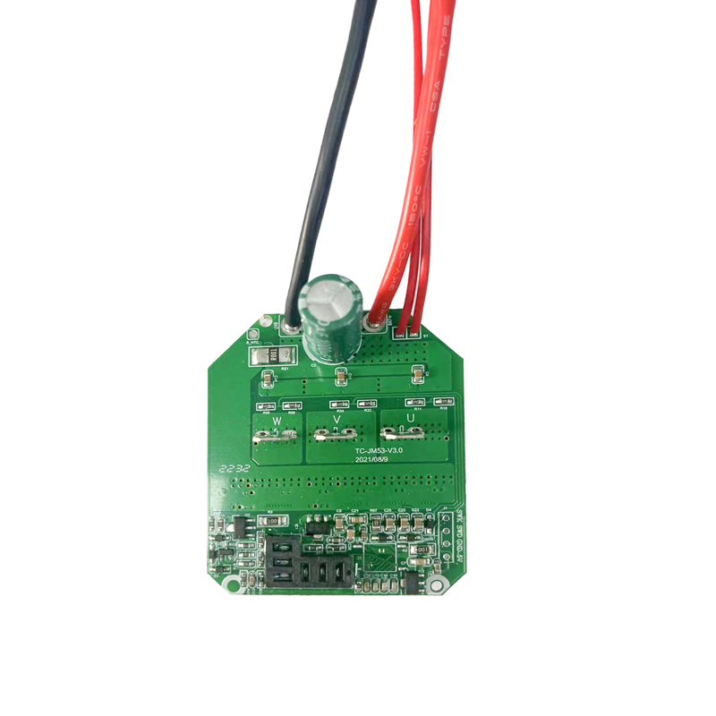
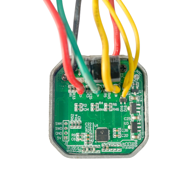
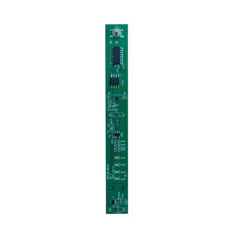
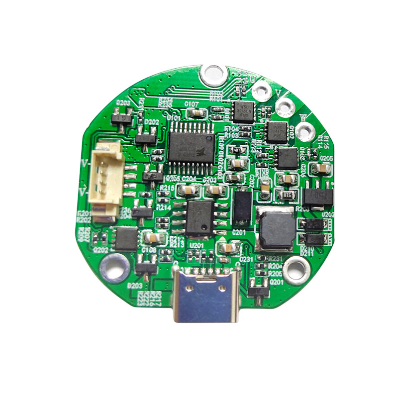
Part2: SMT Processing
Patch introduction
SMT patch refers to the abbreviation of a series of technological processes that are processed on the basis of PCB. PCB (Printed Circuit Board) is a printed circuit board.
SMT is Surface Mount Technology (Surface Mounted Technology) (abbreviation for Surface Mounted Technology), which is the most popular technology and process in the electronic assembly industry. Electronic circuit surface mount technology (Surface Mount Technology, SMT), known as surface mount or surface mount technology. It is a kind of surface mount components without leads or short leads (referred to as SMC/SMD, called chip components in Chinese) on the surface of the printed circuit board (Printed Circuit Board, PCB) or the surface of other substrates. Reflow soldering or dip soldering and other methods to solder and assemble the circuit assembly technology.
Under normal circumstances, the electronic products we use are designed by pcb plus various capacitors, resistors and other electronic components according to the designed circuit diagram, so all kinds of electrical appliances need various smt chip processing technology to process .
SMT basic process
Solder Paste Printing-->Parts Mounting-->Reflow Soldering-->AOI Optical Inspection-->Maintenance-->Sub-Board.
Electronic products pursue miniaturization, and the previously used through-hole plug-in components cannot be reduced. The functions of electronic products are more complete, and the integrated circuits (ICs) used have no perforated components, especially large-scale and highly integrated ICs, which have to use surface mount components. Products are mass-produced and production is automated. The factory must produce high-quality products at low cost and high output to meet customer needs and strengthen market competitiveness. Development of electronic components, development of integrated circuits (IC), and multiple applications of semiconductor materials. The revolution of electronic technology is imperative to follow the international trend. It is conceivable that the development of surface assembly technology and technology such as smt cannot be achieved when the production technology of international cpu and image processing device manufacturers such as intel and amd has advanced to 20 nanometers.The advantages of smt chip processing: high assembly density, small size and light weight of electronic products, the volume and weight of chip components are only about 1/10 of those of traditional plug-in components. Generally, after using SMT, the volume of electronic products is reduced by 40%~60% %, the weight is reduced by 60% to 80%. High reliability and strong anti-vibration ability. Solder joint defect rate is low. Good high frequency characteristics. Electromagnetic and radio frequency interference is reduced. Easy to automate and improve production efficiency. Reduce costs by 30% to 50%. Save material, energy, equipment, manpower, time, etc.
It is precisely because of the complexity of the smt chip processing process that many smt chip processing factories have emerged, specializing in smt chip processing. In shenzhen, thanks to the vigorous development of the electronics industry, smt chip processing achievements the prosperity of an industry.
Process
The basic process components of SMT include: screen printing (or dispensing), placement (curing), reflow soldering, cleaning, testing, rework
1. Silk screen printing: Its function is to leak solder paste or patch glue to the pads of the PCB to prepare for the welding of components. The equipment used is a screen printing machine (screen printing machine), which is located at the forefront of the SMT production line.
2. Dispensing: it drips glue onto the fixed position of the PCB board, and its main function is to fix the components to the PCB board. The equipment used is a glue dispenser, which is located at the front end of the SMT production line or behind the inspection equipment.
3. Mounting: Its function is to accurately install the surface-mounted components on the fixed position of the PCB. The equipment used is a placement machine, which is located behind the screen printing machine in the SMT production line.
4. Curing: Its function is to melt the patch glue, so that the surface mount components and the PCB board are firmly bonded together. The equipment used is a curing oven, which is located behind the placement machine in the SMT production line.
5. Reflow soldering: its function is to melt the solder paste, so that the surface mount components and the PCB board are firmly bonded together. The equipment used is a reflow oven, located behind the placement machine in the SMT production line.
6. Cleaning: Its function is to remove the welding residues such as flux that are harmful to the human body on the assembled PCB board. The equipment used is a washing machine, the location may not be fixed, it may be online or not.
7. Inspection: Its function is to inspect the welding quality and assembly quality of the assembled PCB board. The equipment used includes magnifying glass, microscope, in-line tester (ICT), flying probe tester, automatic optical inspection (AOI), X-RAY inspection system, functional tester, etc. The location can be configured in a suitable place on the production line according to the needs of the inspection.
8. Rework: Its function is to rework the PCB board that has detected the failure. The tools used are soldering iron, rework station, etc. Configured anywhere in the production line.
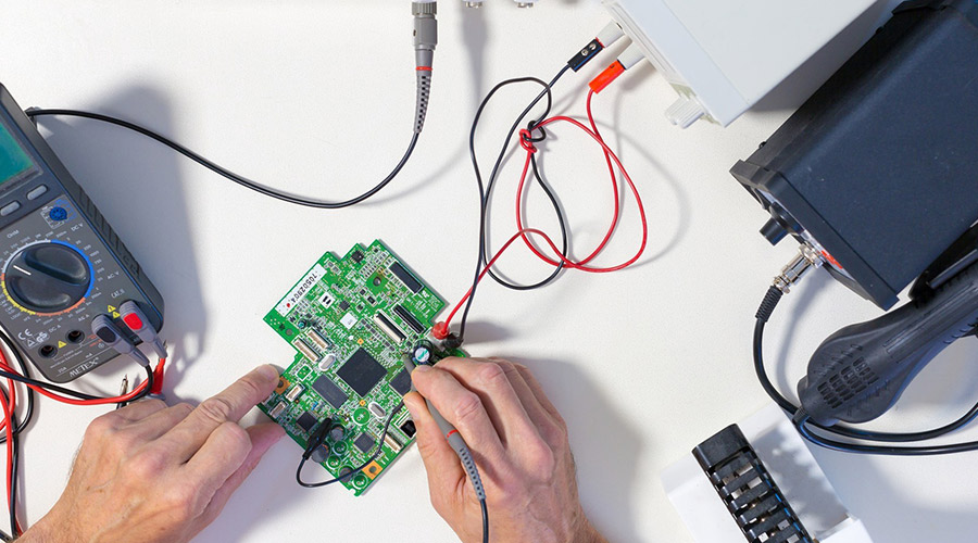
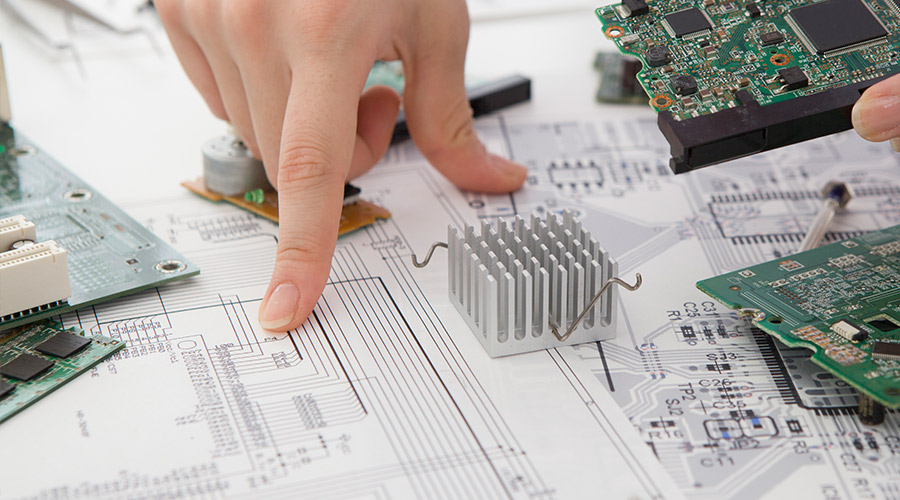
Part3: Functional debugging
1. Power-on observation
Do not rush to measure the electrical indicators after power-on, but observe whether there is any abnormality in the circuit, such as whether there is smoke, whether there is abnormal smell, touching the outer package of the integrated circuit, whether it is hot, etc. If an abnormal phenomenon occurs, turn off the power immediately, and then turn on the power after troubleshooting.
2. Static debugging
Static debugging generally refers to the DC test carried out without adding an input signal or only adding a fixed level signal. The potential of each point in the circuit can be measured with a multimeter, and the potential of each point in the circuit can be measured by a multimeter. Analyze and judge whether the DC working state of the circuit is normal, and find out the components in the circuit that have been damaged or are in a critical working state in time. By replacing components or adjusting circuit parameters, the DC working state of the circuit can meet the design requirements.
3. Dynamic debugging
Dynamic debugging is carried out on the basis of static debugging. Appropriate signals are added to the input end of the circuit, and the output signals of each test point are sequentially detected according to the flow direction of the signals. , and then debug until the requirements are met.
During the test, you can't rely on feelings and impressions, but always observe with the help of instruments.
When using an oscilloscope, it is best to set the signal input mode of the oscilloscope to the "DC" block. Through the DC coupling method, the AC and DC components of the measured signal can be observed at the same time.
Through debugging, finally check whether the various indicators of the function block and the whole machine (such as signal amplitude, waveform shape, phase relationship, gain, input impedance and output impedance, etc.) meet the design requirements, and if necessary, further propose circuit parameters. Reasonable correction.
4.Other work in electronic circuit debugging
According to the working principle of the system to be adjusted, the debugging steps and measurement methods are drawn up, the test points are determined, the positions are marked on the drawings and the board, and the debugging data recording table is drawn.
Set up a debugging workbench, the workbench is equipped with the necessary debugging instruments, and the equipment should be easy to operate and easy to observe.
Students often don't pay attention to this problem. When making or adjusting the machine, the workbench is very messy, and tools, books, clothes, etc. are mixed with the instruments, which will affect the debugging.
Special reminder: When making and debugging, be sure to arrange the workbench clean and tidy.
For the hardware circuit, the measuring instrument should be selected according to the system to be adjusted, and the accuracy of the measuring instrument should be better than that of the system under test.
The debugging sequence of the electronic circuit is generally carried out according to the signal flow direction, and the output signal of the circuit that has been debugged before is used as the input signal of the next stage to create conditions for the final unified adjustment.
When selecting a digital circuit implemented by a programmable logic device, the input, debugging and downloading of the source file of the programmable logic device should be completed, and the programmable logic device and the analog circuit should be connected into a system for overall debugging and result testing.
During the debugging process, the experimental phenomena should be carefully observed and analyzed, and records should be made to ensure the integrity and reliability of the experimental data.